Modern Circuit Design
Read time: 33 minutes (8267 words)
Back in the dawn of time, when electronics was a new technology, designers spent hours wiring up circuits and testing them with a variety of expensive test tools:
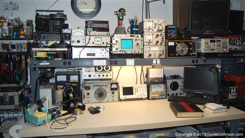
I have a friend who had a bench like this in his basement. He and I built our first computers from parts we scavenged from old electronic gizmos we bought in surplus stores, just for the parts!
When digital circuits first arrived, the parts got much smaller, and you could get sockets to plug them onto a board. Then your job was to wire the pins together to make up your gadget. Unfortunately, with lots of parts, the wiring got very messy!
You could buy all the gear needed to do this at your local Radio Shack (remember those?)
To build something like this, you needed lots of wire, a stripping tool to peel away the plastic coating on the wire, and a soldering iron and solder to fuse the wires to the pins on the sockets where each part would live. Tedious work to say the least.
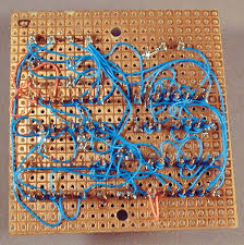
A revolution occurred when someone thought up a way to make a connection to a pin without using solder. Wire-wrap technology looked like this:

Suddenly, things got a bit easier. But boards also got bigger, and this was the result:
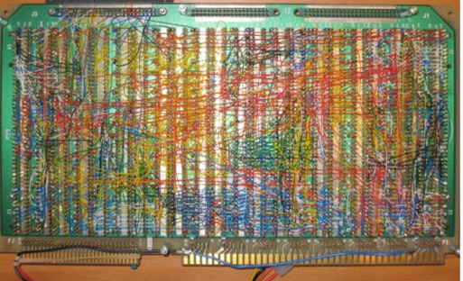
Your eyes went cross-eyed trying to follow each wire to make sure your circuit was wired correctly.
Blue-Flame Testing
Once your design was finished, you hooked it up to a power supply and fired it up! You watched carefully to make sure you saw no flames or smoke rising up from anywhere. This was called the “blue-flame test”. Something like this:
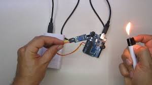
Well, not really, that is an Arduino board hooked up to a temperature sensor, looking for the heat from a yellow flame.
Occasionally, when our boards were a mess, we would want to set fire to them, on purpose!
Digital Circuit Design
George Boole’s Algebra helped in working out the design. Suppose you want to build a Multiplexor, used to route signals . A four-to-one multiplexor would have four input signals, a selector, and one output signal. Setting the selector picks one of those four inputs and sends it along to the output.
You could build one of those using our parts kit in a snap.
We can label our inputs as A,``B``,``C``, and D, and label the output
Q. Since there are four of them, we need two input signals to identify which
one we want. Call those inputs a and b. Here is the Boolean expression
we would need for our circuit:

We can build this entire thing using just simple NAND gates (an AND with an inverter GATE on the output end). Here is the required circuit:
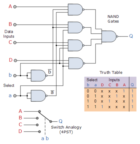
That is a lot of parts. Fortunately, we could buy small DIP packages with four NAND gates in a single part. Still we had a lot of wiring to do!
Programmable Arrays of Gates
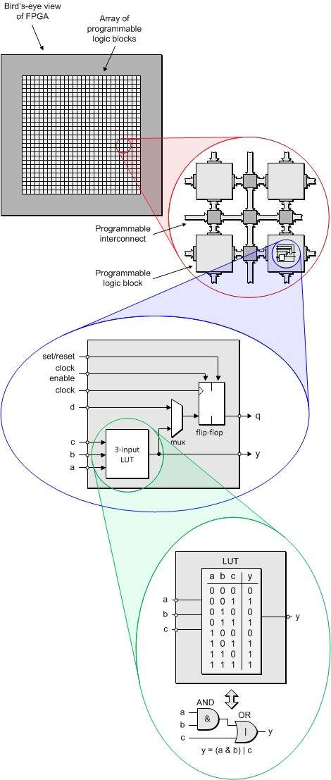
Another revolution occurred when someone, staring at that figure up above, noticed that we were spending a lot of time wiring up something that basically implemented that truth table in the diagram. What if we could simply build such a table in a memory component, load the table with the right bits, then simple “look up” the right answer. No ugly circuit was required.
This led to the development of the “Field Programmable Gate Array” (FPGA)
This cool idea has led to the production of a bunch of boards suitable for designing and testing real digital parts. Here is one of mine:
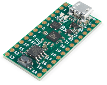
This TinyFPGA board is available form SparkFun for around $38.
IT has the following features:
7680 4-input look-up tables
128KB block RAM
8MB Flash memory
41 user I/O pins
Program over USB with Python tools
Along with the development of tools like this, it also occurred to designers that setting up these gadgets could be done in software, and no more wiring was required. Suddenly software development skills could land you a job in the hardware world!
Language designers came up with “Hardware Description Languages” that looked and felt much like the normal programming languages in use by software developers. There are many such languages around, but two stand out:
VHDL
Verilog
Of these, I prefer Verilog, since it is more closely related to C/C++ programming. Let’s take a peek at Verilog:
Installing Verilog
I am going to show you some examples of modern hardware design using the Verilog HDL language. There is a nice open-source tool called Icarus Verilog available for this language, and it is available for all platforms.
We will use a companion tool, GTKwave, to visualize signals moving around in our design.
Installing it is easy on the Mac:
$ brew install iverilog
$ brew install gtkwave
On your Linux system, do this:
$ sudo apt-get install iverilog
$ sudo apt-get install gtkwave
Hello Verilog
We will not be learning this language in detail, but I will show you enough to use it to prototype some of the parts we need for our simulator. To get started, we need to write the classic “Hello, World” program in Verilog. This is pretty easy:
1 2 3 4 5 6 7 8 | // Verilog Hello, World Demo
module hello();
initial begin
$display ( "Hello, World!" );
#10
$finish;
end
endmodule
|
Now, this code has nothing to do with hardware design, but it does demonstrate how we can make our design generate output to help see what is going on. Plus it satisfies those programming gods who demand that you create a “Hello, World” project in any new language you meet!
Here is a sample run of this program:
There! We have done it! Now we can move on to more interesting examples.
Designing a Counter
Something more useful to explore is a simple counter circuit. Here is a block diagram of the part we want:
We will provide this counter with a 4-bit internal register that increments on
every clock tick. Obviously, it will “roll over” and return to zero once we hit
15 ticks. The “enable” signal will be used to stop incrementing, and the
reset signal will return the counter to zero.
Here is the code:
1 2 3 4 5 6 7 8 9 10 11 12 13 14 15 16 17 18 19 20 21 22 23 24 25 26 | // 4-bit counter
module counter_4b(
clock,
reset,
enable,
count
);
input clock;
input enable;
input reset;
output [3:0] count;
wire clock;
wire reset;
wire enable;
reg [3:0] count;
always @ (posedge clock) begin : COUNTER
if (reset == 1'b1)
count <= #1 4'b0000;
else
if (enable == 1'b1)
count <= #1 count + 1;
end
endmodule
|
And the output:
As it stands now, there will be no output if we run this code. The right way to check the functioning of our component is to wire it up into a test fixture and exercise it. This is not as nice as using Catch for C++ testing, but this is how things are done.
Here is the test code:
1 2 3 4 5 6 7 8 9 10 11 12 13 14 15 16 17 18 19 20 21 22 23 24 25 26 27 28 29 30 31 32 33 34 | module counter_tb();
reg clock, reset, enable;
wire [3:0] count;
initial begin
$display ( "time\t clk reset enable count" );
$monitor (
"%g\t %b %b %b %b",
$time,
clock,
reset,
enable,
count
);
clock = 1;
reset = 0;
enable = 0;
#5 reset = 1;
#10 reset = 0;
#5 enable = 1;
#100 enable = 0;
#10 $finish;
end
always begin
#5 clock = ~clock; // Toggle clock every 5 ticks
end
counter_4b counter (
clock,
reset,
enable,
count
);
endmodule
|
The block of code labeled “initial” is how we set up the system. This assigns initial values to all of our wires and registers. It also sets up timing data used to change various signals ever so many simulation clock ticks.
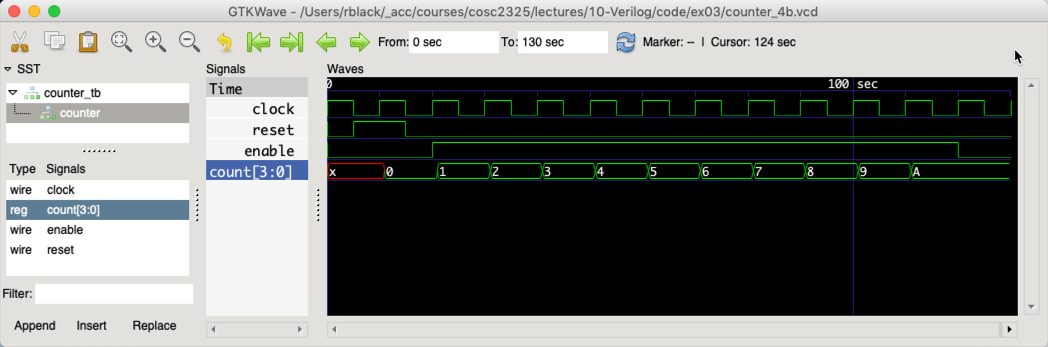
Running this gives this result:
This output can be studied together with the test code to see what is happening. The notation used to set up timing of the signals from the test bench is a bit convoluted, but here is what is happening.
Basically, there is a master simulation clock running when we start a Verilog
program. We set up our clock signal so it changes state every five
simulation ticks. The $monitor statement tells the code to generate an
output line any time one of the indicated signals changes value. We set the
initial values for all signals (except count) in the initial block,
then start generating signal changes as follows:
time = 5, set reset to 1
time = 15, set reset to 0
time = 20, set enable to 1
time = 120, set enable t- 0
time = 120, stop simulation
The #nn is the delay before this action happens.
If you look at the counter code, you will see a #` before the code that
changes the count value``. That means that one tick after either the
reset or enable signals change, we update the count signal.
Does the output make sense? A bit of study will convince you that it is correct.
Visualizing the Signals
Verilog supports generating VCD files (Value Change Dump), which can be
displayed on gtkwave.
Here is a modified version of the code that generates the VCD file, and also displays the output as before. I needed to move things around so the VCD file got generated.
Here is what GTKwave displayed:
This is more like what hardware folks are used to seeing. The cool thing is everything was done n software. We wired up no physical parts, but we see the system running as though it was a real thing!
SimpleCPU
In doing some research on how instructors use Verilog in classes, I found this code from Swarthmore College Digitsl Design course page:
1 2 3 4 5 6 7 8 9 10 11 12 13 14 15 16 17 18 19 20 21 22 23 24 25 26 27 28 29 30 31 32 33 34 35 36 37 38 39 40 41 42 43 44 45 46 47 48 49 50 51 52 53 54 55 56 57 58 59 60 61 62 63 64 65 66 67 68 69 70 71 72 73 74 75 76 77 78 79 80 81 82 83 84 85 86 87 88 89 90 91 92 93 94 95 96 97 98 99 100 101 102 103 104 105 106 107 108 109 110 111 112 113 114 115 116 117 118 119 120 121 122 123 124 125 126 127 128 129 130 131 132 133 134 135 136 137 138 139 140 141 142 143 144 145 146 147 148 | module SimpleCPU(input clk,
output reg [3:0] pc, // Program Counter
output reg [3:0] opCode, // op code
output reg [1:0] src, dst, // src and dst register
output reg [3:0] immData, // "Immediate" data
output reg [3:0] r0, r1, r2, r3, // Registers
output tri [3:0] mBus, dstBus // Buses
);
reg [3:0] pcIncr; // Program Counter Increment
wire [3:0] pcRes; // Output of pc ALU
wire pcz; // Unused - zero flag for pc ALU
reg [1:0] myState; // State (phase of excution)
reg [11:0] myROM [15:0]; // ROM (holds program)
reg [3:0] mbEn, dbEn; // Used to determine which tri-state buffers are
// enabled for master bus and destination bus.
reg [2:0] aluOp; // Determines if ALU adds or subtracts
reg [3:0] aluOut; // Register to hold output of main ALU
reg zFlag; // Zero flag
wire [3:0] resVal; // Output (combinational) of ALU
wire zVal; // Output (combinational) of ALU zero flag
include params.vh
// define the initial program counter and control state
initial
begin
pc = 4'b0000;
myState = fetch;
end
always @(posedge clk)
case(myState)
fetch:
begin
{opCode, src, dst, immData} = myROM[pc];
myState <= decode;
end
decode:
begin
case(opCode)
movi, addi, subi, cmpi, bitandi, bitori:
begin
mbEn <= bEn_Imm;
end
mov, add, sub, cmp, bitand, bitor, bitnot:
case(src)
Rg0: mbEn <= bEn_R0;
Rg1: mbEn <= bEn_R1;
Rg2: mbEn <= bEn_R2;
Rg3: mbEn <= bEn_R3;
endcase
endcase
case(dst)
Rg0: dbEn <= bEn_R0;
Rg1: dbEn <= bEn_R1;
Rg2: dbEn <= bEn_R2;
Rg3: dbEn <= bEn_R3;
endcase
case (opCode)
sub, subi, cmp, cmpi: aluOp <= opSub;
add, addi: aluOp <= opAdd;
bitand, bitandi: aluOp <= opAnd;
bitor, bitori: aluOp <= opOr;
default: aluOp <= opNot;
endcase
myState <= exec;
end
exec:
begin
case(opCode)
addi, add, subi, sub, cmpi, cmp,
bitnot, bitandi, bitand, bitori, bitor:
begin
pcIncr <= 4'd1;
mbEn <= bEn_ALU;
aluOut <= resVal;
zFlag <= zVal;
end
jmp: pcIncr <= immData;
jz: pcIncr <= zFlag ? immData : 4'd1;
jnz: pcIncr <= zFlag ? 4'd1 : immData;
default: pcIncr <= 4'd1;
endcase
myState <= store;
end
store:
begin
case(opCode)
movi, mov, add, addi, sub, subi,
bitnot, bitandi, bitand, bitori, bitor:
case(dst)
Rg0: r0 <= mBus;
Rg1: r1 <= mBus;
Rg2: r2 <= mBus;
Rg3: r3 <= mBus;
endcase
endcase
pc <= pcRes;
myState <= fetch;
end
endcase
assign mBus = (mbEn==bEn_R0) ? r0 : hiZ;
assign mBus = (mbEn==bEn_R1) ? r1 : hiZ;
assign mBus = (mbEn==bEn_R2) ? r2 : hiZ;
assign mBus = (mbEn==bEn_R3) ? r3 : hiZ;
assign mBus = (mbEn==bEn_Imm) ? immData : hiZ;
assign mBus = (mbEn==bEn_ALU) ? aluOut : hiZ;
assign dstBus = (dbEn==bEn_R0) ? r0 : hiZ;
assign dstBus = (dbEn==bEn_R1) ? r1 : hiZ;
assign dstBus = (dbEn==bEn_R2) ? r2 : hiZ;
assign dstBus = (dbEn==bEn_R3) ? r3 : hiZ;
mk2ALU dataALU(aluOp, mBus, dstBus, zVal, resVal);
mk2ALU pcALU(opAdd, pc, pcIncr, pcz, pcRes);
endmodule
module mk2ALU(input [2:0] op,
input [3:0] src, dst,
output ZFlag,
output [3:0] res);
parameter opSub=3'b000, opAdd=3'b001, opAnd=3'b010,
opOr=3'b011, opNot=3'b100;
assign res = (op == opSub) ? (dst - src) :
(op == opAdd) ? (dst + src) :
(op == opAnd) ? (dst & src) :
(op == opOr) ? (dst | src) :
~src;
assign ZFlag = !(res);
endmodule
|
I am working on this code to clean it up a bit for further study.
Here is the processor this code implements:
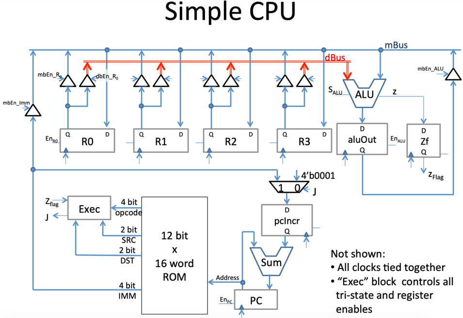
Obviously, this is not the same machine we are building. but based on what oyu know now, you should be able to see how it works!