Arduino Processor
Read time: 14 minutes (3573 words)
We have been studying a tiny chip, the attiny85 which is small enough to
embed in just about any commercial gadget you might think of. However, with
only eight pins, two of which need to supply power, the number of devices you
can interact with is pretty limited. Still it is a useful chip.
We will be working with its bigger brother for the rest of the class. The
atmega328p, found on most Arduino boards, is a much more versatile chip!
This chip has many more I/O pins available, but the instruction set is almost
identical to the set we studied for the attiny85. There are a few new
instructions available, but not so many we need to worry much about the
differences.
CPU Structure
Here is the internal structure of the chip we will use:
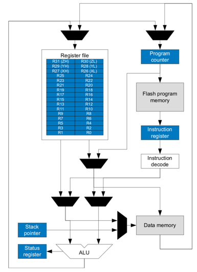
Nothing too exciting here, based on our studies.
What makes this chip very useful is the system of supporting gadgets the manufacturer places around this chip.
Block Diagram
Here is a block diagram showing our new processor:
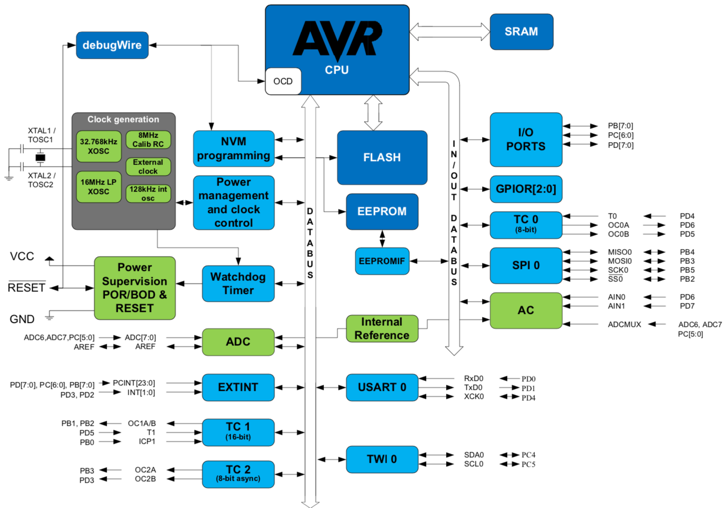
This diagram is showing the components that surround the actual CPU which is that blue block at the top! All of these parts are inside the chip, but provide an interface to useful internal tools, and allow for connections to the outside world. Basically, the result is a complete “system on a chip” a popular term in today’s marketplace.
Much of what we will do for the last part of this course is look at how we hook up a computer to gadgets that interact with us humans! We will explore using assembly language to access these gadgets, either to control them, or to read signals coming from them.
Processor Data Sheet
Here is the “data sheet” for the AVR chip we will be modeling. We will examine the instruction set in this processor, but not much about its electrical properties. We will also learn a bit about some interesting internal additions to the processor that make working with hardware easier.
Mapping Arduino Pins to AVR I/O pins
The Arduino board was designed for hobby use, not professional development. The ecosystem set up for Arduino shields the user from much of what we have been learning in this class. The biggest hassle we face is figuring out how to attach a physical gizmo to the Arduino board.
If you look closely at the Arduino board, you will see numbers near the place where a connection can be made (those black sockets on either side of the board. There are some devices, called “shields” in Arduino land, that simply plug into those sockets covering the entire board. For our work, we will use the breadboard next to the Arduino board to attach some devices, then use “jumper wires” to make a connection from one of the Arduino connector sockets to the breadboard to create a simple circuit we can play with. We will go over that in class.
When we write code for the processor on the board, we will focus on the I/O
“port” defined in the chip. The chip will refer to those ports using pin
designations you see in the data sheet. Something like PORTB, Pin5, or
PB5. The Arduino board runs a wire on the printed circuit board PB5 to
one of its connector pins, and calls that “Digital Pin13”. Much of the
reference material you will see on the Internet will refer to those Arduino
numbers, and you need to figure out what chip pin they are talking about.
Here is a diagram that will be very useful. In spite of saying it is for the
ATmega168, the pin designations also apply to the ATmega328p, which is
what we will focus on.
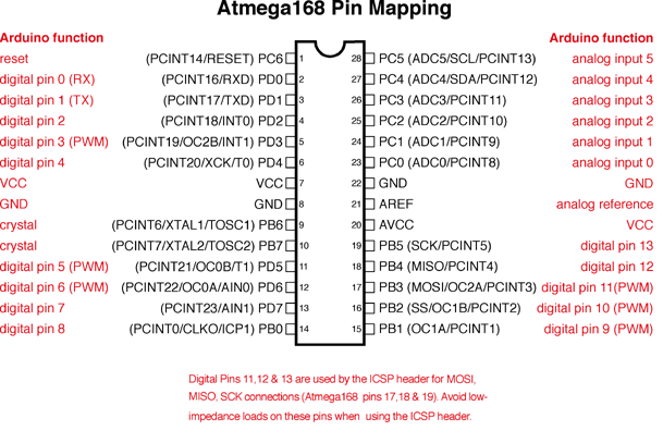
This should be enough to get started in our explorations.
Remember that you already looked at a simple AVR assembly project, the
avr-blink project. We will move on next, and explore the internal alarm
clock on the chip!